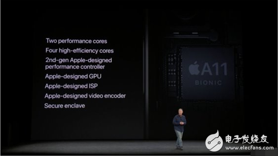
The Apple A11 Bionic Chip contains a series of processing cores and powerful controllers designed for specific tasks. We don't know much about this processor, and with the launch of the new iPhone, today we can finally deepen its GPU, neural engine, 6-core CPU, NVMe SSD controller and new custom video encoder. To understanding.
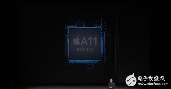
New 3-core GPU
This is the first time Apple has integrated its own custom GPUs in its A-series chips. Compared to the ImaginaTIon GPU, which is the leader in smartphone graphics architecture, the former has increased its speed by 30%.
Apple's new GPU is not only faster, but also more energy efficient. At the same workload, it consumes half the power of the A10 Fusion processor.
Originally, the industry developed GPUs to accelerate graphics. For many years, it has also begun to undertake other mathematical operations with similar repetitive properties, so it is also called "General Purpose GPU." Apple originally developed OpenCL as an API to implement GPGPU, but later they have integrated GPGPU computing into the Metal API, which is optimized for GPUs in iOS and Mac devices. At the WWDC in June this year, the Metal API has been updated to the Metal 2 version.
Now that Apple is designing its own graphics chip and managing its chips, we can expect the development of GPU and GPGPU to be faster. In addition, Apple is also studying machine learning, which is one of the best tasks of the GPU. Machine learning builds models only on a set of known things, and then uses this "knowledge" model to find things that identify matches. For example, the known thing is a photo of various flowers, then it can use the model to find something that might be a flower in a new photo or camera viewfinder.
Apple only said that the new GPU has three cores and does not provide other detailed technical information about the new GPU design. Different GPU designs need to be optimized for specific tasks and strategies. These designs also make the core definitions very different, so you can't directly use Apple's GPUs and GPUs from Intel, NVIDIA, AMD, Qualcomm, ARM Mali, and others. The contrast of meaning.
TBDR
It is worth noting that Apple said that the A11 biochip GPU graphics architecture is based on TIL Based Deferred Rendering. TBDR rendering technology is designed for mobile devices with limited resources. It effectively renders only scenes visible to the human eye in 3D scenes. The IMR immediate rendering mode of the desktop PC GPU (and Qualcomm Adreno and ARM Mali mobile GPUs) is implemented without discrimination, and the portion of the masking process will still be rendered by the processor, which also leads to more meaningless read and write operations. A lot of performance and bandwidth is wasted, and mobile GPUs generally cannot accept this simple and rude way.
TBDR skips what the user can't see, divides the scene into different blocks, analyzes which blocks need to be rendered, saves performance and bandwidth, and has faster block memory and lower latency. This process allows it to execute vertices and fragments asynchronously, which helps to make better use of the entire GPU. Apple pointed out that performing vertices usually requires a lot of fixed-function hardware, and mathematical operations and bandwidth are required to execute fragments. Full overlap allows the device to utilize all of the hardware blocks on the GPU at the same time.
As a technology, TBDR has a close relationship with ImaginaTIon's PowerVR. The latter chose a more distinctive approach, parallel development with the desktop GPU, emerged in the first generation of the iPhone, is a perfect GPU architecture optimized for mobile platforms, its energy efficiency has the advantage that PC GPU can not match.
However, although ImaginaTIon said this spring, Apple has not proved that they have not infringed on Imagination knowledge products, but now Imagination seems to no longer say that Apple's new GPU uses any unlicensed PowerVR technology. On the contrary, Imagination is now difficult to protect itself. After the absence of Apple’s order, the situation turned sharply. Recently, it was reported that they had sold themselves.
In addition, although there are not many successful GPU architectures (many attempts end up failing), TBDR is not completely unique to Imagination. This is the same as the CPU industry. Although many competitors try to break the status quo, the current mobile device CPU is still dominated by the ARM architecture. PCs and servers are still dominated by Intel's x86 architecture.
Apple's Metal 2 provides developers with the details of TBDR so developers can optimize memory usage and provide finer-grained synchronization for the GPU to do more. Apple also said that the new GPU has features that greatly enhance TBDR, allowing third-party applications and games to reach a new level of performance and functionality.
Quad-core ISP neural engine
The development of a new GPU architecture "is not so creative," so the A11 biochip's graphics signal processor ISP also has a new neural engine that can solve a variety of specific tasks, such as matching, analyzing and calculating camera sensor image data. Thousands of reference points.
These tasks can actually be done by the GPU, but the network engine has been specifically optimized for matrix multiplication and floating point processing, so it is especially good at handling these tasks.
The network engine itself has two parallel cores that can be used to process real-time, and can execute 600 billion operations per second. In other words, in addition to being able to use complex effects on photos like the previous generation ISP, it can also be used for live video. In addition to using various effects, it also allows the camera system to recognize objects and structures in the scene to track and focus on the object the user is currently shooting.
The network engine is also the source of the name of the A11 biochip. "Bionic" usually means that people get motor and electronic devices to enhance biological functions, that is, because of these enhancements, they have superhuman ability. For the A11 biochip, you can understand it in reverse. It is actually a machine that gains human-like enhancements. You can also understand this: for those who use this chip, it is a bionics enhancement that allows users to accomplish tasks that are not possible with a typical robot.
6 new CPU cores, second generation performance controllers
The third focus of the A11 biochip is the ARM architecture CPU core designed by Apple. Apple has introduced the custom A4 SoC since 2010 and has quickly refined its design in the following years. In 2013, the first 64-bit ARM A7 chip was introduced, and industry competitors were dumbfounded.
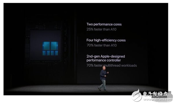
Last year's A10 Fusion was born from a new architecture. It is actually composed of two high-performance cores and two energy-efficient cores. Two sets of CPU cores with different performances can be solved very well. The role played is significantly different, more to balance the performance and performance. Simply put, the hardware-level manager built into the A10 allows the chip to better manage, organize, coordinate, and distribute tasks on the device, deciding how to allocate based on maximum processing power or energy-saving task requirements. The use of the CPU core.
This year, Apple pointed out that their second-generation performance controllers can perform tasks on a lower-energy core, or speed up processes on a faster high-performance core, and even allow the entire 6-core CPU to be fully powered. Using an asymmetrical multitasking design, the A11 biomimetic chip can activate any number of cores proportionally, depending on the task to be processed.
Processing multiple tasks on multiple cores requires more than just multiple cores on the SoC. Application and OS features also need to be designed to take advantage of these cores. In fact, many years ago, before the advent of the iPhone, Apple had such a targeted design at the operating system level, as did third-party developers in Apple.
Apple has detailed their software operating system strategy: shutting down unnecessary processor units and effectively sequencing the processes so that their scheduling operations can be as fast and efficient as possible. A similar strategy is now adopted in chip hardware. Other mobile device vendors, such as Samsung and LG, will never develop their own PC OS platform.
From the beginning, Google has adjusted Android to the direction of portable mobile platforms, which is not suitable for users who have performance requirements. Google doesn't really have a tablet or desktop computing business. The mobile platform is also aimed at mobile phones with an average selling price of less than $300. The price of Android One is $100, which is quite competitive. Android buyers are actually an audience for advertising, not for complex features such as UI, application performance or multitasking support. Android apps are also optimized for easy ad serving.
A11 two performance-optimized general-purpose CPUs have a 25% improvement in speed compared to last year's A10, and the energy-efficiency core has been improved. The A11 energy-efficiency core has increased to 4 and the speed has increased by 70%.
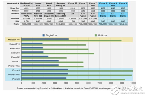
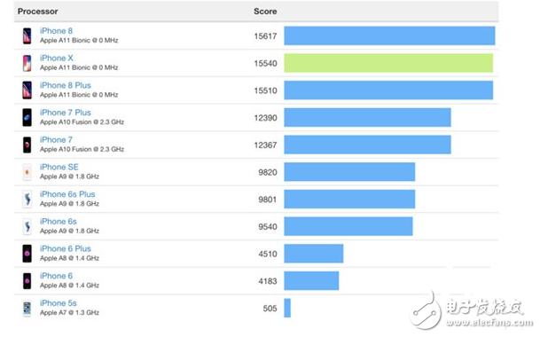
Geekbench runs in the same way, the iPhone 7 and iPhone 8 of the same configuration have obvious differences, the single core speed is 25% faster than the former and 80% faster than multicore.
This deserves special mention, because Apple's chip also has a new neural engine, GPU, camera ISP and other functions, beyond the scope of the general processor running test.
Samsung has been marketing their eight-core processors for many years. However, the contrast between Samsung processors and Apple is too clear. Samsung's single-core is actually slow, and the operating system is not optimized to effectively utilize multi-core performance. Google even claims that the Nexus 7 has 16 cores (the sum of CPU and GPU cores), but the marketing is always just marketing, and the device won't be a bit faster. In fact, not only does the device not get faster at all, but as the usage time increases, the performance of the device continues to decrease.
Compared to various boasting marketing, Apple highlights the performance of the product in practical applications, such as the A11 bionic chip optimized for 3D games and AR experience.
In addition to the CPU, Apple also designed Secure Enclave in A7 to store sensitive data. Apple said that the A11 biochip has improved in this regard, but did not elaborate.
SSD, secure storage
There are other special features in the A11 biochip, such as the ultra-fast SSD memory controller that integrates custom ECC algorithms. This is not just for speed. Johny Srouji, senior vice president of hardware technology at Apple, said: "Users purchase equipment, and the storage durability and performance should be consistent with the equipment."
That is to say, the data (files, applications and photos) stored on the device can be better protected, avoid errors or storage failures, reduce the risk of losing memory and files, and avoid inexplicably slowing down after using the device for a period of time. problem. This is a common problem with many Android devices.
Apple pioneered the custom NVMe SSD storage controller on the 2015 MacBook to optimize SSD read and write at the hardware level. Then introduce this technology into the iOS device in the A9 chip. The NVMe was originally developed for the enterprise market, not for consumer electronics. Because there is no suitable solution to add NVMe controllers to mobile phones, there are cheaper, off-the-shelf (sometimes) protocols that can access SSD storage. Apple developed it on its own.
A11 uses Apple's third-generation iOS storage controller, but there are so many things to introduce, and Apple did not introduce it at the press conference.
New Apple Video Encoder
Two years ago, Apple A9 brought a hardware-based HEVC decoder that enabled devices to play H.265 / High Efficiency video content. A hardware encoder was introduced in the A10 last year to support the iPhone 7 to create and save content in that format.
iOS 11 also supports these new features and adds the corresponding "Efficient Video Capture" option to the camera settings. With this option turned on, the photo will be in HEIF format and the video will be compressed using HEVC format.
The advantage of these High Efficiency formats is that they greatly reduce the space occupied by high-pixel photos and video.
Apple said that the 1K 4k 30fps video size in the HEVC format is 170MB, and the H.264 format has the same video size of 350MB, which is twice the former.
To play these HEVC video content naturally requires a device that can decode them. iOS devices before A9 can be soft-solved, but compared to hard solutions, the software takes longer and consumes a lot of power.
HEIF video can be converted to H.264 video, or the user can default to "mostly compatible" to continue saving images in JPG format and saving video in H.264 format. But this also means disabling 4K 60fp (and 24fps movie settings) to record video.
Apple developed a proprietary video encoder for the A11, and it also made this point public. It’s really interesting! Previously on the iPod and other devices, Apple directly used the industry's existing standards to integrate support for a variety of audio and video codecs, including Microsoft's WMA, WMV and VC-1. Instead of activating this kinetic energy, Apple chose to use industry standards developed by MPEG LA partners.
We don't know if Microsoft is getting Windows Media IP's license for Apple's chips. But the bigger question is that Apple needs to pay for what they don't want to use. Now that Apple develops its own video encoders, they only need to optimize for the supported formats, not all the codecs that the chip vendor chooses.
Google’s YouTube was originally working with Apple to provide H.264 video content to iOS users. However, Google intends to improve the VP8 and VP9 codecs they acquired from On2. While YouTube continues to offer H.264 video to iOS users, YouTube videos do not have H.264 format or updated H.265/HEVC format, so Safari users cannot view 4K YouTube videos on the web.
So you will see that Apple TV 4K can't play YouTube 4K content either. This is actually because Google doesn't provide content that Apple TV 4K can decode. I still don't know how Apple and Google will solve this problem. Does Google continue to refuse to provide 4K support for iOS devices?
With the integration of efficient, purpose-optimized HEVC encoders in iPhone 7, iPhone 8 and iPhone X, users need less space to store more photos and videos. It is conceivable that this can also reduce the wear and tear of the SSD storage, because about half of the things will be written, moved and then suddenly erased.
HEVC also supports recording higher frame rate content. iPhone 8 and iPhone X support recording 4K 60fps video. Although the 4K video recorded on the iPhone 7 is also very clear, if the camera or the subject moves too fast during recording, the picture will appear jittery. Support for 60fps frame rate, the video will look better.
However, the better the frame rate, if there is no advanced compression technology, a one-minute video may occupy 800MB space. With HEVC, 4K 60fps video does not have much more space than 4K 30fps video. Here to remind users, HEVC 60fps video requires powerful processing power or a dedicated hardware decoder to play. The old Mac playing 4K video recorded on iPhone 7 has been very difficult.
Although we have introduced so much about the A11 biochip, there are still many undisclosed secrets in this chip.
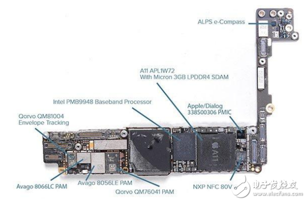
Disassemble the internal structure of the iPhone8A11 processorThe iPhone 8, iPhone 8 Plus and iPhone X both use the Apple A11 Bionic processor. What is the internal structure of this processor that can achieve 2+4 core super performance? Recently, the professional chip disassembly research website disassembled the iPhone 8 Plus and looked at the construction of the A11 processor.
TechInsights (a research organization merged with Chipworks in 2016) made a detailed disassembly of the iPhone 8 Plus. Chipworks has repeatedly dismantled the iPhone deconstruction processor and other chip configurations. After the merger with TechInsights in September 2016, two Continue to disassemble the iPhone together. After disassembling the iPhone 8 Plus, it was found that the Apple A11 Bionic processor is 30% smaller than the Apple A10 Fusion, because the A11 uses a more advanced 10nm process and the size of the iPhone X motherboard, resulting in a smaller area.
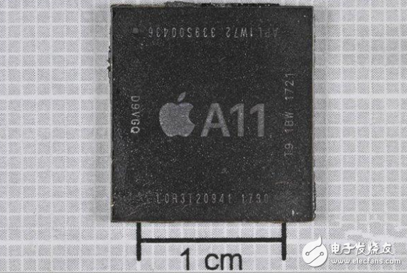
The A11 processor has 6 cores, 2 cores and high efficiency 4 cores. Even if the area is reduced, the processor still has a complicated structure. The picture from TechInsights shows that the 6 cores of the A11 processor are distributed on the right side of the whole chip, 2 CPU1. It is an efficient processing core with a large footprint. Four CPU2s are power-saving processing cores with a small area. In summary, the processing core accounts for 15% of the A11 processor area.
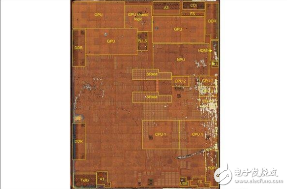
The A11 processor is the image processing core, which accounts for 20% of the area. It has 6 cores and is similar in position to the A10 Fusion processor.

iPhone 8 Plus motherboard chips kicked one by one
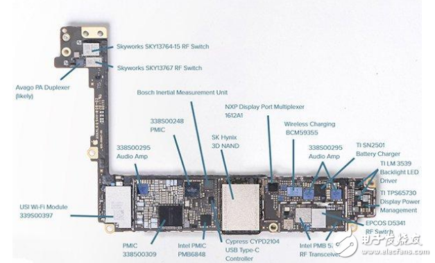
In addition to the A11 processor, TechInsights also took pictures of the front and back of the iPhone 8 Plus motherboard. On the back of the A11 processor are SK Hynix's 3D NAND flash memory chip and BCM59355 wireless charging chip, while the A11 processor On the one hand, Micron 3GB LPDDR4 SDRAM and NXP are distributed. One thing to note is that Apple and Qualcomm have a lawsuit relationship. The iPhone 8 Plus tries to get rid of Qualcomm and uses Intel chips in both Baseband and LTE.
Distribution Cable,Fiber Optic Cable,Mulitifiber Fiber Optic Cable,Distribution Optical Cable
ShenZhen JunJin Technology Co.,Ltd , https://www.jjtcl.com