This article brings you a detailed tutorial on cadence allegro pcb layout.
First, use Design Entry CIS (Capture) design schematic 1, create a projectFile--"new--"project; enter the project name, specify the project placement path;
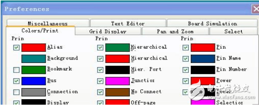
2, set the operating environment OpTIons--"Preferencses:Color: colors/Print
Lattice: Grid Display
Miscellaneous: Miscellaneous
Often take the default value
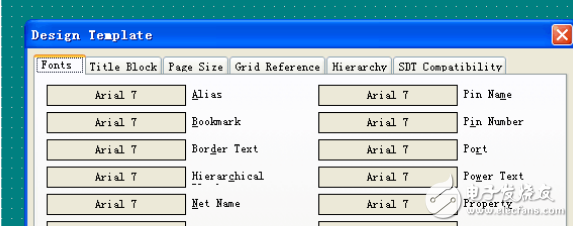
Set template: OpTIons--"Design Template: (apply to new map)
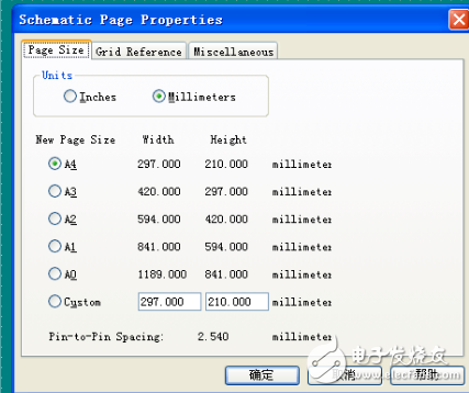
Set the current drawing OpTIons--"SchemaTIc Page Properities
File--"New Library --" select the project to add to
Design --"New Part. (or right-click on the Library and select New Part)
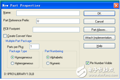
(1) Homogeneous: In a composite package component (when multiple component diagrams are composed) each component diagram is the same (default applies to standard logic)
(2) Heterogeneous: different component diagrams used in composite package components (when multiple component diagrams are composed) (more suitable for large components)
A package diagram of multiple components in a package, switching the view component package with a View ext part (previous part):
(1)place --"line  Draw a line to draw the package shape;
(2)place--"pin  Place the pins; put one or more;
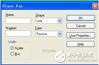
Different types of pins are selected differently;
5, draw the schematic(1) Place the appliance
Place--"part; can choose from the design cache, the living component library, the software comes with the component library; select Add Library to add the component library;

Power and ground (power gnd) are selected from the right toolbar;
(2) Connection line wire
Bus: must be connected to the wire by a branch line and correspond to the net alias (wire:D0, D1...D7;bus:D[0..7]) data bus and data bus lead-out line Must define net alias
( 3) Schematic new page (multiple pictures possible:
Connection between single-level circuit diagrams with the same name "circuit port connector" off-page connector
Multi-level circuit diagram: replace the circuit diagram of the actual circuit with a block diagram (hierarchical block.). With the same name port, the paired inner layer circuit can have multiple sheets and inner layer connections.
(4) PCB layer pretreatment
Edit component properties
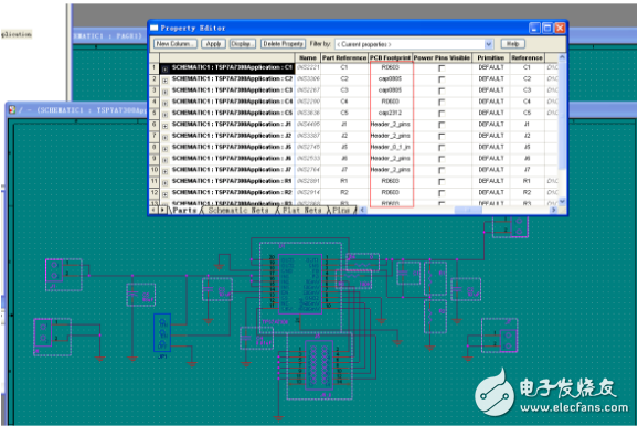
Before importing the PCB, you must correctly fill in the component assignment (PCB Footprint) parameters (frame multiple components, then Edit Properties), the property editor appears as shown; edit pcb footPrint (with components in allegro pcb The package name is consistent; part Perference is the name of the component after the netlist is imported into the allegro pcb; other attributes can be edited; other required attributes can also be added;
(6) Classification attribute editing
Edit Properties--"New ColumnClass: IC (IC, IO, Discrete, classified in the PCB) Place the definition room (Room) Edit Properties--"New ColumnRoom Add text and images
Add text, bitmap (Place..)
6. Subsequent processing of schematic drawing(Switch to the Project Manager window, select the *.DSN file, and then post-process - DRC check, generate netlist and component list)
(1) Design rule check (Tools--"Design Rules Check..)
Design Rules Check
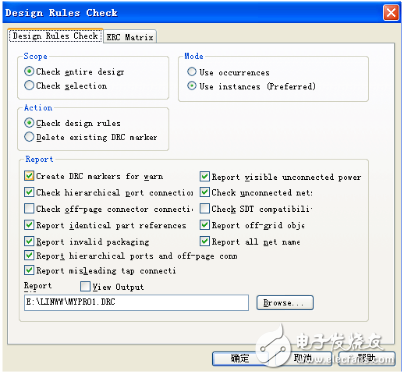
Scope (scope): entire (all) / selection (selected)
Mode: events (event: entity circuit that appears multiple times in the same entity in the same drawing page) instance (entity: component symbol in the drawing page) Action: check design rules/delete DRC Report:
Create DRC markers for warn Check hierarchical port connection Check off-page connector connection Report identical part referenves Report invalid part referenves Report invalid package (check for invalid packages)
Report hierarchical ports and off-page connector (listing port and off-page connectors) Check unconnected net Check SDT compatible Report all net names
(2) Component auto-numbering (Tools -- "Annotate")
Scope (scope): Update entire design/selection
Action: Incremental reference update
Unconfitional reference update
Reset part reference to “?†Reset the number to “?â€;
Add/delete Intersheet Reference (number of the port on the pagination sheet plus/delete the number of the drawing) Reset reference numbers to begin at 1 each page schematic each page reset number starts from 1
(3) Automatically update the properties of the device or network (Tools--"Update Properties..)
7, generate a netlistAfter the schematic check is correct
Tools--Create NetLists generates netlists;
A two-dimensional line scanner, comprising a scanner body and a bracket, characterized in that: the scanner body is composed of a handle, an upper cover and a rear cover respectively fixed at the front and rear ends of the handle, and the front side of the handle is The interior is provided with a light-transmitting part, a light-guiding part, a main board, and a key board. The light-guiding part is also provided with a dust-proof mirror frame embedded with a dust-proof lens at the bottom. The main board is plugged and fixed with copper on one side. A two-dimensional decoding board is installed and fixed on the copper column, and a two-dimensional code component is connected below the two-dimensional decoding board. On the button position, the rear side of the handle is internally provided with a wire clip assembly formed by the upper half of the wire clip and the lower half of the wire clip. The wire clip assembly is placed on the corresponding square groove inside the back cover, and the wire The wire on the clip assembly extends to be connected with the main board, the bracket is composed of a bracket rod, a bracket head and a bracket base respectively fixed on the top and bottom of the bracket rod, and the bracket rod is composed of a left bracket rod and a right bracket rod. The center of the bracket base is provided with a circular groove which is convenient for the bracket rod to be inserted and connected, and the scanner body is hung on the bracket head through the handle.
2D Wired Scanner ,Usb Barcode Scanner,Wired Barcode Scanner For Ipad,Zebra Wired Barcode Scanner
ShengXiaoBang(GZ) Material Union Technology Co.Ltd , https://www.sxbgz.com