In order to facilitate placement and production, it is desirable that surface-mount components be packaged in a CAD library to determine their zero-degree orientation and positioning reference in accordance with uniform regulations. The zero direction of the component pad pattern is in principle required to be consistent with the orientation of the device in the packaging. The packaging herein refers mainly to the packaging of the disc. If the direction is inconsistent, it needs to be performed in the procedure of the placement equipment one by one. If there is any omission in the amendment, it will cause a bad situation.
What needs to be pointed out here is that devices with a relatively large amount of resistance, capacitance, and inductance must comply with this rule because the amount used is too large. If there is a problem, the amount of work required for verification and modification during production is also large. For designers, it only takes a lot of work, but if it is solved in production, it may be a day or two. As for ICs and other devices, one-on-one checks must be conducted during production, as long as they follow the unified rules. The positioning criteria of the components, the unified requirements must be the center of the component body.
This is because the placement equipment is the central point of the placement center of the component, and in the automatic recognition and positioning, the data is corrected and compensated based on the center of the component body. In actual production, it has been found that individual designers use the center of the first leg of the component as the positioning reference of the component. In this case, the production process cannot be discovered in advance, and can only be discovered during the production process. Once it occurs, only Can be modified on the production line, one by one data, imagine that if there are thousands of components of the coordinates must be modified one by one, equipment engineers will be crazy. Some products with more complicated circuits may be designed and deployed by several engineers. At this time, it must be noted that the used pad pattern library must be unified. If everyone builds their own library, there will be problems with the final product. Once encountered in Beijing this situation, there is a communication company that produces a big smart phone, there is a product we find to produce, in production, found that the same packaged device, in different areas of the circuit board, the zero direction of the component is Differently, it was learned through communication that this circuit board was designed collaboratively by several people. Of course, this situation is relatively rare, but it also hopes to attract attention.
The following are the requirements for the common component land pattern library for reference:
1, chip components (non-polar) resistance, capacitance, inductance

The zero direction is 1 foot on the left, the center of the component body is used as the reference point, and the tantalum capacitor

The zero direction is negative on the left and the center of the component body is used as a reference point
3, diode

The zero direction is the negative pole on the left, and the center of the component body is the reference point 4. Inductance

Zero-degree direction is 1 foot on the left, using the center of the component body as a reference point
5, cylindrical diode

The zero direction is negative on the left and the center of the component body is used as a reference point
6, SMD aluminum electrolytic capacitors
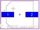
The zero direction is positive on the left and the center of the component body is used as a reference point
7, SOT23 package
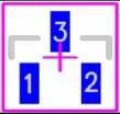
The zero degree direction is 1 foot at the bottom left and the center of the component body is used as the reference point. 8. SOT25 package
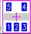
The zero degree direction is 1 foot at the bottom left, using the center of the component body as a reference point
9, SOT343 package
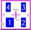
The zero degree direction is 1 foot at the bottom left, using the center of the component body as a reference point
10, SOT223 package
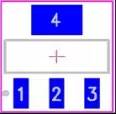
The zero degree direction is 1 foot at the bottom left, using the center of the component body as a reference point
11. T0252 (DPAK) Package

The zero degree direction is 1 foot at the bottom left, using the center of the component body as a reference point
12, SOIC, SOP, SSOP package

The zero degree direction is 1 foot at the bottom left, using the center of the component body as a reference point
13, TSOP package

The zero degree direction is 1 foot at the bottom left, using the center of the component body as a reference point
14, SOIC J pin

The zero degree direction is 1 foot at the bottom left, using the center of the component body as a reference point
15, QFP package
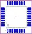

The zero degree direction is 1 foot at the bottom left, using the center of the component body as a reference point
16, PLCC package
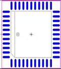
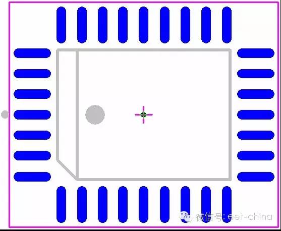
The zero direction is 1 foot in the left center, using the center of the component body as a reference point
17, QFN package

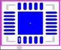
The zero degree direction is 1 foot at the bottom left, using the center of the component body as a reference point
18, BGA package
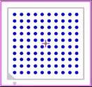

The zero degree direction is 1 foot at the bottom left, using the center of the component body as a reference point
For other types of devices, refer to the above principles.
D-sub Connector Contacts
A D-sub connector is a form of connector commonly found in electronic and computer systems. It consists of a D shaped metal band and two or more parallel rows of either pin contacts (male) or socket contacts (female). D-sub connector contacts can vary in size, material, current rating, length and resistance.
The most common type of connector is the crimp contact. These are assembled by inserting a stripped wire end into the cavity at the rear of the contact. The cavity is then crushed using a crimp tool, gripping the contact to the wire.
What are D-sub connector contacts used for?
The D-sub connector contacts carry the signal from the source to the destination across the D–sub connection.
Types of D-sub connector contacts
Most D-sub connectors are supplied with contacts ready in place. Contacts can be replaced if damaged or if the application of the D-sub connector is to be changed from the original design specification.
High-current, high-voltage, or co-axial inserts require larger contacts. The material of the D-sub connector contact can be changed if the robustness or quality of the connection needs to be improved.
D-SUB coaxial contact,D-Sub Connectors Contacts,D-Sub Plug Connectors Contact,D-Sub Receptacle Connectors Contact
ShenZhen Antenk Electronics Co,Ltd , https://www.antenkelec.com