Banknote clearing is an important business of the bank. At present, the banknote sorting machines used by many domestic banks are imported from abroad and are expensive. There are few domestic banknote sorting machines, and their functions are very limited. It is difficult to meet the requirements of high-speed real-time performance. In particular, the banknote sorting machine that can identify banknotes by image processing has just started.
To this end, a banknote identification system was designed. The system uses DSP as the core processor, combined with image sensor CCD and complex programmable logic device CPLD, and is equipped with high-performance analog-to-digital converter AD9200 to collect and process banknote images. The system mainly identifies nine banknotes of RMB 4, 10 yuan, 20 yuan, 50 yuan and 100 yuan in the fourth and fifth editions of RMB, using digital image processing technology and improved self-organizing map neural network (SOFM) extraction. The length, width, and direction block characteristics of the banknote image distinguish the face value, front and back, and forward and reverse of the banknote. The final system can achieve higher recognition speed and recognition rate.
1 hardware designThe overall hardware structure of the identification system is shown in Figure 1. The image of the renminbi is first scanned by the sensor CCD to obtain the photoelectric conversion signal, and is amplified by AMP three times; then the amplified analog signal is converted into a standard digital signal by the analog-to-digital converter AD9200, and sent to the CPLD buffer; finally through the EDMA The channel is input to the RAM of the DSP, and the image is processed and recognized in the DSP. The signal logic timing of the entire system is controlled by the CPLD. In addition, there are some auxiliary links, such as banknote input and output devices, user detection devices, reset devices, and the like.

Figure 1 Block diagram of the overall hardware structure of the identification system
The collection of banknote images consists of a CCD and an A/D converter. This system adopts linear array CCD [1], which has faster sampling speed, simple circuit design, small size and easy timing. According to the system's requirements for acquisition speed, the horizontal resolution is set to 4 pixels/mm, and a total of 800 pixels are collected; the vertical resolution is 1 pixel/mm. The height of each image is no more than 76 mm, there is a certain interval between the two banknotes, and 100 columns are actually collected. Thus, the pixels of each image are 800 & TImes; 100. The judgment of the entry and exit of the banknote is detected using an infrared photocell.
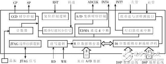
After the image of RMB is acquired and A/D converted, it is temporarily stored in the CPLD chip XC95144, and then directly transmitted by the DSP through the EDMA channel. The timing signals for the entire acquisition and storage process are generated by the XC95144. The internal structure of the CPLD that needs to be programmed is shown in Figure 2. The ADCLK signal is a clock signal sent to the AD9200, and the SP and CP signals are transmitted to the shift register of the CCD as a start pulse and a sampling clock pulse.
The identification part of the image is composed of a digital signal processor DSP [2] and corresponding peripheral circuits, and its structure is shown in FIG. The digital signal processor DSP selects the TMS320C6711GFN150 chip produced by TI Company, and the main frequency is 150MHz. The scanned banknote image data Data is stored in the static memory SRAM by EDMA, and the DSP performs a series of recognition algorithm operations on the data stored in the SRAM, and outputs the final result through the McBSP1 port of the DSP.

Figure 2 Internal structure of the CPLD

Figure 3 Structure diagram of DSP and corresponding peripheral circuits
Face Plate,electrical face plates,cat6 faceplate,face plates
NINGBO UONICORE ELECTRONICS CO., LTD , https://www.uniconmelectronics.com