Flexible electronic technology is an emerging science and technology. Emerging electronics based on flexible and ductile substrates are known as flexible electronics. Due to its unique flexibility and ductility, flexible electronic systems have broad application prospects in many aspects.

Flexible electronics
Flexible Electronics, also known as Plastic Electronics, Printed Electronics, Organic Electronics, Polymer Electronics, etc.; is the production of organic/inorganic materials in flexible/ Emerging electronics on ductile plastic or thin metal substrates.
In people's minds, organic materials, such as plastics, are good insulators, and few people think that plastics can also conduct electricity. In recent years, due to new breakthroughs in the study of conductive polymers, organic materials can be changed from conventional insulators to conductive semiconductors, and flexible electrons have emerged. The development of modern chemistry and other technologies has promoted the development of a discipline such as flexible electronics.
The key to flexible electronics manufacturing includes manufacturing processes, substrates and materials, etc. The core of which is micro- and nanopatterning, involving multidisciplinary research in mechanics, materials, physics, chemistry, electronics, etc.
Flexible electronics, with its unique flexibility/ductility and efficient, low-cost manufacturing processes, have broad application prospects in information, energy, medical, defense and other fields, such as flexible electronic displays, organic light-emitting diodes (OLEDs), printed RFID, and thin-film solar panels. , electronic newspapers, skin patches (skin patches) / artificial muscles.

In addition to integrating electronic circuits, electronic components, materials, flat displays, nanotechnology and other fields, flexible electronics can assist traditional industries such as plastics across industries such as semiconductors, packaging and testing, materials, chemicals, printed circuit boards, and display panels. The transformation of industries such as printing, chemicals and metal materials will increase the added value of the industry. Therefore, the development of flexible electronic technology will bring revolutionary changes to the industrial structure and human life.
Flexible electronic technology is a brand new electronic technology revolution that has attracted worldwide attention and has grown rapidly. The US Science magazine listed the progress of organic electronic technology as one of the world's top ten scientific and technological achievements in 2000, alongside major discoveries such as the Human Genome Sketch and Cologne Technology. American scientist Alan Hage, Alan Mark Deermid, and Japanese scientist Shirakawa Hideki won the 2000 Nobel Prize in Chemistry for their pioneering work in the field of conductive polymers.
The difference between flexible electronics and traditional electronics manufacturing
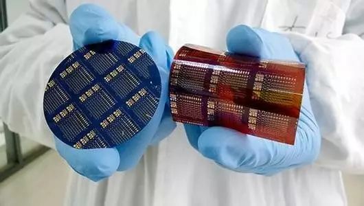
At present, the electronics industry basically belongs to the traditional semiconductor industry. The equipment used in manufacturing is quite large, and the cost is high, and the manufacturing efficiency is low. The whole concept of flexible electronics is to print traditional semiconductor products, components and circuits. Alternative. The difference between flexible electronics and traditional electronic circuits is mainly from three aspects:
(1) Application prospects
Once a very soft substrate is applied to the design or the line is made invisible or foldable, it is quite different from a conventional hard substrate.
(2) Manufacturing costs
The roll-to-roll printing process is used, and the problem of wasting more than 95% of materials like lithography is avoided in the use of materials, and the area printed by printing is equivalent to the area used, and its usage rate is 90%. Above, in terms of long-term development, the printing method will be much lower than the cost of traditional lithography; silicon CMOS wafers are generally costing 10$/cm2, composite semiconductors are even more expensive, and the ideal cost of flexible electronics is 0.1$/ Cm2, from the cost can be seen the great advantages of flexible electronics.
(3) Investment perspective
Traditional semiconductor factories are going to have billions or even billions of investment, but the printing method is like traditional printing. As long as the investment is tens of millions, the basic scale can be established. It should be emphasized that the ink used for printing is different from the traditional printing, and needs special development. The initial cost of development is relatively high due to the small amount, but the cost after mass production becomes lower.
Structure and materials of flexible electronic systems
Although flexible electronic technology can be applied to different fields, its basic structure is similar, including at least the following four parts: electronic components, flexible substrate (fflexible substrate), cross-linked conductor (finterconnect) and adhesive layer.
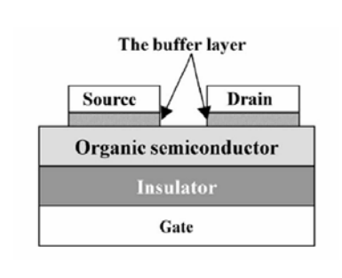
Flexible electronic system structure
The four main parts of the flexible electronic system structure are described below.
1, electronic components
Electronic components are the basic components of flexible electronic products, including thin-film transistors, sensors, etc. commonly used in electronic technology.
These electronic components are not fundamentally different from the components of traditional electronic technology. Some components use inorganic semiconductor materials (such as silicon). Because of their brittle materials, they are prone to brittle fracture during deformation, so they are usually not directly distributed in the circuit. On the board, it is placed on a rigid cell island, and then the micro-cell islands carrying the components are redistributed on the flexible substrate. This has the advantage of protecting the electronic components and avoiding them. Damaged during bending. Of course, some electronic components can also be directly distributed on a flexible substrate, such as a partial thin film transistor, due to its own characteristics, can directly withstand a certain strain without affecting its function.
Compared with traditional microelectronics technology, the use of organic electronic components is a prominent feature in flexible electronic technology, among which organic thin film transistors (organic thin film tran-sistor, OTFT) occupy a very important position, the use of organic materials In order to reduce the weight and thickness of components, it has created conditions for improving flexibility and ductility.
2, flexible substrate
Flexible substrates are the most prominent places where flexible electronics technology differs from traditional electronics. It has the common characteristics of the traditional rigid substrate, the first is the insulation: the insulated flexible substrate ensures that the electronic equipment will not leak during use, ensuring that it can work normally and ensure the safety of its use.
Secondly, the higher strength: no matter which kind of electronic technology, the role of the substrate is equivalent to the role of the skeleton, and without the high strength to ensure, it can not guarantee its normal use.
Once again, it is cheap: the substrate material is one of the most used materials in the circuit, and only the use of inexpensive materials can effectively reduce the cost of electronic products.
In addition to the common features of the above substrates, flexible substrates have their own unique characteristics. The first is flexibility: the flexibility of flexible electronic systems is mainly manifested through the substrate, and different materials can be used for products with different flexibility requirements; for example, electronic skin is usually made of very flexible silicone resin (Si1icone), and flexible Electronic displays have lower flexibility requirements than electronic skin, and polyethylene terephthalate (PET) is commonly known as polyester.
Secondly, it is thin film: although it is called a substrate, it is no longer a "plate" in size, but a film; the substrate of a flexible electronic system is usually about 1mm, which reduces the cost of materials and reduces the weight of the product. .
In view of the above considerations, flexible substrates are ideal for the use of high molecular polymers. Currently available flexible substrate materials include DuPont's Kapton Polyimide (PI) film materials, polydimethylsiloxane, polyethylene terephthalate (PET), etc. It can meet the requirements of insulation, flexibility and strength.
3, cross-linked conductor
The electronic components are first distributed on the rigid micro-cell islands, and a plurality of such micro-cell islands are redistributed on the flexible substrate. These micro-cell islands do not exist independently, and they are connected by cross-linking conductors to form A complete flexible circuit, that is to say a cross-linked conductor, acts as a wire in a flexible electronic system. The crosslinked electrical conductor is attached to the flexible substrate in the form of a metal film.
4 adhesive layer
The combination of the various components of a flexible electronic system requires an adhesive layer, and the bonding layer is particularly important for the bonding of the crosslinked electrical conductor to the flexible substrate.
The adhesive layer of a flexible electronic system should have the following characteristics:
(1) Heat resistance.
In the process of assembly and use of flexible electronic products, it is inevitable to experience an environment higher than normal temperature, and certain heat resistance is necessary.
(2) Binding power.
Since flexible electronic products are constantly subjected to tensile and bending deformation during use, the two thin layers connected by the adhesive layer usually have different mechanical properties. If the bonding force is not large enough, the relative sliding of the two thin layers is inevitably caused. Stripped.
(3) Bending ability.
The adhesive layer itself is an integral part of the flexible electronic system structure, and its own bending ability has an important influence on the bending ability of the entire structure. At present, the adhesive layer materials commonly used in flexible circuits are mainly acrylic resin and epoxy resin.
5, the cover layer
The cover layer (also known as the encapsulation layer) mainly protects the flexible circuit from dust, moisture or chemicals, and also reduces the strain on the circuit during bending. Recent studies have shown that the cover layer can be reduced in the flexible circuit. The stress intensity of the edge of the rigid micro-cell island fcellisland and its delamination from the flexible substrate can be suppressed.
According to the characteristics of the flexible electronic system, the cover layer is required to withstand long-term deflection, and therefore the cover material is the same as the substrate material, and the fatigue resistance must meet certain requirements. In addition, the cover layer covers the sub-etched circuit and is therefore required to have good conformability to meet the requirements of bubble-free lamination. Common materials for the cover layer are acrylic resin, epoxy resin, polyimide, and the like.
Preparation process of flexible electronic system
As with traditional IC technology, manufacturing processes and equipment are also the main drivers of the development of flexible electronics. The level of flexible electronic manufacturing technology includes chip feature size and substrate area size. The key is how to manufacture flexible electronic devices with smaller feature sizes on a larger format substrate at a lower cost.
Flexible electronics manufacturing processes typically include: Material Preparation → Deposition → Patterning → Packaging, which can be integrated by roll-to-roll (R2R) substrate transport.
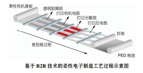
Flexible electronics manufacturing focuses on production costs, production efficiencies, achievable feature sizes, and compatibility of organic materials. In recent years, flexible electronic manufacturing technology has been greatly developed due to breakthroughs in active materials and their patterning technologies. .
The core of flexible electronics manufacturing is the fabrication of thin film transistors (TFTs). The key manufacturing technology is to create high-resolution patterning technology for channel length between source and drain, which directly affects device performance such as output current and switching speed. In the process, it is particularly necessary to eliminate parasitic leakage and reduce crosstalk to ensure a high switching ratio. Most applications require an organic thin film transistor (OTFT) channel length of less than 10 μm. Existing patterning techniques include lithography, shadow masks, Printing (microcontact printing and printing), etc. The specific comparison is shown in the table below.
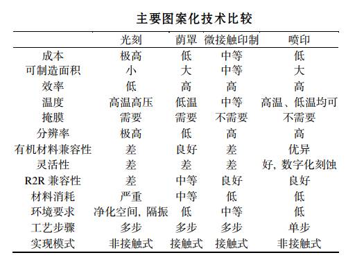
Energy beam technology such as lithography is widely used in the patterning of microelectronic devices, and its resolution is high. However, due to its complicated process, expensive equipment, solvent and developer cannot be used for plastic substrates, it is time-consuming and expensive, and is only suitable for The small area is patterned, the environment is demanding when etching the underlayer, the activity of the organic electronic material and the polymer substrate are destroyed when the photoresist is removed, and it is limited in flexible electronic manufacturing applications.
The shadow mask technology is a "dry" process that avoids solvent damage to organic semiconductors but with limited resolution.
Printing technology simultaneously implements functional material deposition and patterning in the same step. The main methods are: (1) transferring and pasting the complete circuit onto a flexible substrate, such as transfer (stamp); (2) directly on the flexible substrate Prepare circuits such as jet printing and microcontact printing (soft etching).
In the transfer method, the entire structure is first prepared on a silicon wafer or a glass plate by standard photolithography, and then transferred to a flexible substrate to produce a high-performance device. Due to the application of photolithography and high-temperature deposition technology, the transfer technology can only be manufactured. Small area devices with high processing costs.
Micro-contact printing enables the creation of multi-level patterns for masking, which can be integrated with R2R batch manufacturing technology. Usually one master can make more than 100 stamps, each stamp can achieve more than 3000 stamps, stamps The cost is relatively low, and the 60 nm high-resolution pattern can be produced at a speed of several centimeters per second, but it is difficult to realize multi-layer patterns. Micro-contact printing can be used for a variety of materials such as amorphous silicon, polysilicon and TMOS, but it is difficult to directly use Etching organic materials. Lan Hongbo et al. conducted a detailed discussion and analysis on the research progress and development trend of nanoimprint etch dies technology.
The ideal patterning process for flexible electronics should meet: low cost, large area, batch process, low temperature, "plus", non-contact, real-time adjustment, three-dimensional structure, easy multi-layer registration, printable organic/inorganic Materials, etc. As can be seen from the table above, printing is a non-contact, pressure-free, non-printing printing and copying technology. It has the characteristics of non-printing digital printing, and the solution is directly written to realize digital flexible printing at room temperature. Simplifies the manufacturing process. The use of solubilized semiconductor and metal materials to replace traditional vacuum deposition materials can effectively reduce costs. Printing also has the following advantages:
(1) Pattern quality is not limited by lithographic focal length, and can be patterned on non-planar surfaces or even deep trench structures
(2) Good compatibility with organic/inorganic materials;
(3) Direct use of CAD/CAM data processing devices for large-area dynamic alignment and real-time adjustment;
(4) As a non-contact patterning technology, it can effectively reduce defects, and can compensate for defects such as interlayer deformation and misalignment by using a virtual mask;
(5) Print-on-demand (DOD) technology without physical masks;
(6) Fast design and processing of complex 3D microstructures, and rapid changes to graphics through a software-based print control system.
Flexible electronics applications
Along with the development of flexible electronic technology, various electronic products have emerged. Just as microelectronics provides a technology platform for large-scale integrated circuits and computer chip technologies, flexible electronic technology provides a new technology platform for the development of new products. Flexible electronic products are currently in the initial stage of research and development, and some products have been put on the market. From the current research and development trends, flexible electronic technology has a wide range of applications in the following three areas.
1, flexible electronic display
Flexible electronic display is a new product developed on the flexible electronic technology platform. Unlike traditional flat panel displays, such displays can be repeatedly bent and folded, thus bringing great convenience to our lives.
For example, all visuals, including a variety of books, newspapers, magazines, and video files, can be presented on this display and viewed anytime, anywhere. Although the current popular MP4 players and personal digital assistants (PDAs) can meet such use requirements, their displays cannot be bent and folded, and can only be read and viewed on a small screen. And video, visual effects are greatly limited. In contrast, flexible electronic displays have unparalleled advantages. They are like newspapers, they are unfolded when needed, and they are curled or even folded after use, ensuring full portability while ensuring portability.
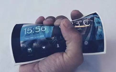
Samples of flexible electronic displays have been successfully developed, and it is believed that it is not far from entering the market. It is worth mentioning that flexible electronic displays use more lightweight organic materials instead of inorganic materials, so their weight is lighter than traditional displays, which is beneficial to improve portability. In addition, the use of polymeric organic materials offers the potential to reduce costs. In addition, the flexible electronic display has the characteristics of thin thickness, and its thickness can be much smaller than that of the currently popular liquid crystal display, so another name of the flexible electronic display is a paper-like electronic display.
2, thin film solar panels
Thin film solar cel1 is another specific application of flexible electronic technology. In today's world, energy has become a topic of global concern, and China is not only facing energy shortages, but also facing environmental pollution. As a clean energy source, solar energy can effectively alleviate the contradiction of energy shortage under the premise of zero pollution in the environment.
As the most common way to use solar energy, solar panels can cover a large area at the lowest cost and effectively utilize solar energy. At present, thin film amorphous Sili-Con solar panels have been successfully developed and marketed.
Thin-film solar panels based on flexible electronic technology can meet the needs of high-power generation, such as the use of thin-film solar panels in solar power plants in sunny desert areas.
In addition, you can make full use of its flexible and lightweight features to integrate it on your clothes. Wearing this kind of clothing to walk or exercise in the sun, the power of small appliances (such as MP3 players and laptops) that are carried around can be supplied by the thin film solar panels on the clothes, thereby achieving the goal of saving and environmental protection.

3. Application background of flexible electronics in the field of RFID
Radio Frequency Identification (RFID) technology is widely used in production, logistics, transportation, medical, food, anti-counterfeiting, etc., without the need for manual contact to complete information input and processing, fast and convenient operation, and rapid development. Radio frequency identification systems usually consist of a transponder and a reader.
The electronic tag is one of many forms of transponders, and can be understood as a transponder of a film type structure, which is convenient to use, small in size, light in weight, and can be embedded in a product. More and more electronic tags will be used in future RFID systems.

The construction situation of electronic tags is moving toward a light, thin, small, and soft direction. In this respect, flexible electronic devices have advantages that are unmatched by other materials. Therefore, the future development of electronic tags in radio frequency identification systems is likely to be combined with flexible electronic manufacturing, making the use of RFID electronic tags more extensive and convenient. In addition, it can also greatly reduce costs and bring higher benefits. This is also one of the future development directions of flexible electronics manufacturing.
Making low-cost flexible electronic tags has two implications. On the one hand, it is a beneficial attempt to make flexible electronic devices. Electronic circuits and electronic devices are moving in the direction of “light, thin, small, and softâ€, and the development of flexible electronic circuits and electronic devices is more noticeable.
For example, a flexible circuit board that can now be produced is a circuit that contains delicate wires and is made of a thin, compliant polymer film that can be applied to surface mount technology and can be bent into a myriad of desired shapes.
The flexible circuit using SMT technology is thin and lightweight, and the insulation thickness is less than 25 microns. This flexible circuit can be bent arbitrarily and can be bent into a cylinder to make full use of the three-dimensional volume.
It breaks the mindset of the traditional intrinsic use area and thus forms the ability to make full use of the volume shape, which can greatly increase the effective use density and form a high-density assembly form in the current method. Comply with the development trend of “flexibility†of electronic products.
On the other hand, it can accelerate the process of recognition and development of radio frequency identification technology in China. In radio frequency identification systems, transponders are the key to technology. Electronic tags are one of many forms of RFID transponders, and flexible electronic tags are more suitable for more occasions. The reduction of the cost of electronic tags will greatly promote the truly widespread application of RFID technology.
4, electronic skin
Another important application of flexible electronics is the electronic skin. Electronic skin, also known as skin-like electrons, is characterized by integrating various electronic components on a flexible substrate to form a skin-like circuit board, which has high flexibility and elasticity like skin, and can be used for many others. electrical equipment.
For example, in the robot technology, the electronic skin can be widely applied: the electronic skin integrates various sensors and electrical conductors, and converts the external force or heat into an electrical signal and transmits it to the computer of the robot for signal processing, so the electronic skin is Called sensitive skin.
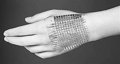
The two most basic features of electronic skin can be summarized as:
1) Flexibility and flexibility like a human skin so that the robot can be as flexible and agile as a real person.
2) The sensor is distributed on the electronic skin so that the robot can feel the change of the external environment keenly.
At present, research on electronic skin at home and abroad is in the ascendant. The sensor, the important electronic component of the robot skin, has made some progress in its principle and application research. The design method of electronic skin based on infrared sensor improves the robot's ability to sense the unknown environment in order to avoid obstacles in time.
In addition, it solves the problem of signal fusion of many sensors in electronic skin. Because PVDF piezoelectric film has high piezoelectricity, flexibility, thinness, light weight and close to the characteristics of human skin, research on electronic skin sensors around this material is common at home and abroad.
Foreign research on electronic skin related issues has also made considerable progress. Japanese researchers have not only developed the theory of electronic skin, but also produced experimental products. In order to study the force perception problem of electronic skin, the possibility of implementing force sensing is discussed by establishing the relationship between force and sensor capacitance.
Although the basic principle of electronic skin is not complicated, how to cover the electronic skin with the robot is quite challenging, because the electronic skin is the external environment that feels the whole body of the robot, and must be integrated. At the same time, the electronic skin exists as an external part. The possibility of damage due to external factors. When the whole or part of the electronic skin is damaged, it needs to be replaced in time.
In response to this demand of electronic skin, the concept of electronic skin unit module is proposed, and each unit module is connected by serial bus, thereby realizing the unity of electronic skin integrity and scalability. However, the use of electric wires inevitably increases the weight of the electronic skin, and the insulating rubber layer of the electric wire also restricts the softness of the electronic skin to some extent.
In this case, an in-depth study of the connecting conductor of the electronic skin has been made, and a new technique in which a metal (gold) film is attached to pre-stretched polyethylene terephthalate, commonly known as a polyester substrate, has been proposed. Experiments have shown that this metal film can still conduct electricity under double tensile deformation (ie, strain up to 100%).
Research on electronic skin sensors is currently mostly focused on sensing (eg, force) of a single external information. However, as an electronic skin, the sensing of multiple external information is very important, that is, external stimuli such as force, temperature, humidity, etc. can be felt at the same time. To achieve this goal, at least three technical breakthroughs are needed:
(1) Material selection: The realization of sensor sensing function depends to some extent on the functional properties of sensor materials, such as piezoelectricity, pyroelectricity or semi-conductivity, so the research and application of functional materials affects sensor technology. development of.
(2) Processing of multiple sensitive signals: A complete (robot) electronic skin is packed with a considerable number of sensory micro-elements, each of which has the function of responding to the external environment, and in some cases each feeling The micro-element also responds to multiple signals (such as simultaneous sensitivities and heat). In the case of a very large amount of signal, how to process the signal to determine the robot's countermeasures against external stimuli is an important issue.
(3) Optimization of electronic skin mechanical properties: As an important application of flexible electronic technology, electronic skin must meet the flexibility of strength assurance; the lightest quality optimization design without damage is also an important consideration.
In addition to robots, electronic skin can also be applied to artificial organs, such as artificial hearts for the treatment of heart diseases, which of course imposes more stringent requirements on the materials of electronic skin. In short, the electronic skin fully utilizes the structure of the flexible electronic system to be lightweight and flexible, and has broad application prospects.
Along with the development of flexible electronic technology, various electronic products have emerged. Just as microelectronics provides a technology platform for large-scale integrated circuits and computer chip technologies, flexible electronic technology provides a new technology platform for the development of new products.
Online Expansion Of Lithium Ion Battery
25Ah Modules Battery,Bluetooth App Battery,Remote Monitoring Battery,Custom Lithium Battery
Wolong Electric Group Zhejiang Dengta Power Source Co.,Ltd , https://www.wldtbattery.com