The frequency synthesizer is the core device in the transmitting system and the receiving system. It adopts phase negative feedback frequency control technology, has good narrow-band carrier tracking performance and bandwidth modulation tracking performance, and provides local oscillator signal for phase up and down conversion, phase noise and The spurs have a good suppression effect, and the frequency source realized by the phase-locked frequency synthesis technology has been widely used in radar, communication, electronics and other fields.
This paper introduces the GPS signal source design as a reference, and introduces the typical application of ADI's frequency synthesizer ADF4360-4 in GPS signal source design.
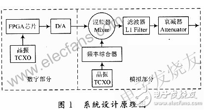
1 Signal source system composition 1.1 System designAccording to the literature, the structure characteristics of GPS signals are known. The purpose of designing GPS signal sources is to simulate the GPS signals transmitted by satellites, that is, baseband modulation of GPS signals and generate GPS RF signals with a frequency of 1 575.42 MHz. According to the literature, in the system. In the overall design, the super-heterodyne up-conversion idea is adopted. According to the system design features, the digital circuit and the analog circuit are divided into two parts. The system design is shown in Figure 1. The digital circuit part is designed with the idea of ​​software radio, and the GPS chip is used to complete the GPS signal. Baseband modulation and intermediate frequency modulation, output 8 b GPS digital intermediate frequency signal, converted to analog signal by D/A device and sent to analog circuit; analog circuit part is the core of the overall design, mainly for the design and implementation of RF circuit board The frequency synthesizer, the mixer and the like are used for mixing, filtering, power control, etc., and the GPS intermediate frequency signal is mixed and modulated to the radio frequency signal, and the up-conversion function is completed by using the radio frequency circuit.

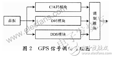
(1) Digital circuit: The digital circuit part is the baseband/IF module design. It adopts the software radio idea. According to the literature, the GPS chip is used to generate GPS navigation message (D code), C/A code and digital intermediate frequency carrier, and baseband modulation is performed on them. The spread spectrum modulation outputs the GPS digital intermediate frequency signal, wherein the GPS signal modulation principle is as shown in FIG. 2, and is mainly composed of a C/A code module, a D code module, a DDS module, and a modulation module. The C/A code module generates a C/A code sequence of the i-th satellite at a rate of 1.023 MHz, the C/A code has 1 023 chips, and the duration is 1 ms; the D code module generates the i-th rate of 50 Hz. Satellite navigation message (D code); DDS module generates digital carrier signal with rate of 12.5 MHz; modulation module performs spread spectrum modulation and BPSK modulation on C/A code, D code and carrier signal, and outputs 12.5 MHz GPS digital intermediate frequency signal .

(2) Analog circuit: According to the literature, the analog circuit part is the RF module design. The frequency synthesizer, mixer, filter and attenuator are used to design the RF circuit. The basic principle is shown in the simulation part of Figure 1. The GPS signal is moved from the intermediate frequency to the radio frequency, filtered by the filter, and the GPS RF signal is output after the power is adjusted by the adjustable attenuator to complete the up-conversion function.
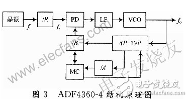
2 frequency synthesizer ADF4360-4 2.1 working principle and its performanceThe main function of the frequency synthesizer is to provide local oscillator signals for system up-conversion. It is mostly used in transmitter and receiver system design, usually by digital phase detector (PD), loop filter (LF), voltage controlled oscillator ( VCO) and a programmable counter (R counter and N counter), etc., digital phase detector (PD) phase comparison of the output signals of the R calculator and the N counter to obtain an error voltage, through the loop filter (LF) The post-controlled voltage controlled oscillator (VCO) produces the desired frequency.
The frequency synthesizer ADF4360-4 is a high-performance phase-locked frequency synthesizer chip produced by Analog Devices. It is a dual-mode pre-frequency-divided single-loop frequency synthesizer that can effectively improve the frequency synthesizer without changing the frequency resolution. Output frequency; its main performance is, the output frequency range is 1450 ~ 1750 MHz, selectable two-way, the output signal frequency is 725 ~ 875 MHz when selecting the two-way frequency; the working voltage is 3 ~ 3.6V; the power of the output signal can be The control range is -13 to -4 dBm; the programmable dual-mode prescaler has a division ratio of 8/9, 16/17, 32/33; it can perform analog and digital lock detection; the VCO is integrated inside the chip. . The working principle of the ADF4360-4 is shown in Figure 3. P/(P+1) is a high-speed dual-mode prescaler with a frequency division modulus of P+1 and P. A is a 5-bit pulse swallow programmable counter. , B is a 13-bit main programmable counter, R is a 14-bit programmable reference divider, and MC is a mode control logic circuit. The device uses a programmable 5-bit A counter, a 13-bit B counter, and a dual-mode prescaler (P/P+1) to determine the main division ratio N (N=BP+A), a 14-bit programmable reference. The R frequency divider divides the external crystal oscillator to obtain the reference frequency fr=f0/R. Therefore, the design only needs to add a loop filter and select an appropriate reference value to obtain a stable frequency output. The output frequency is f0. =fi/R(A+BP), where fi is the input frequency and is provided by an external crystal.

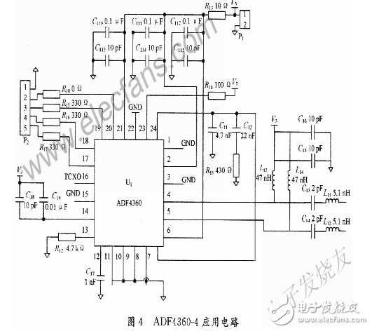
In the analog circuit RF module, the frequency synthesizer ADF4360-4 provides the local oscillator signal for the mixer. The application circuit is shown in Figure 4. The analog input of the frequency synthesizer is the external temperature-compensated crystal oscillator. The crystal oscillator passes the standard through a filter. The clock is sent to the 16-pin REFin of the ADF4360-4; the output pin of the frequency synthesizer is 4: RFoutA and 5-pin RFoutB, these two output differential high-frequency signals are fed into the mixer through the matching network and the resonant filter network. The differential input terminal; the 17th to 19th pins are respectively the CLK pin, the DATA pin, and the LE pin of the control data when the synthesizer is initialized, and are connected with the 20-pin MUXOUT for the test output to a 5-pin plug for the FPGA chip. Connection, as its input and output control interface; 12-pin Cc is the compensation pin, connected to a capacitor ground; 13-pin Rset is used to set the maximum current of the charge pump output, the current size is determined by the formula ICPmax=11.75/Rest, in this circuit Rest=4.7 kΩ; 14-pin CN is connected to Vvco decoupling with a capacitor; 6-pin VCO power supply, 21-pin digital power supply and 2-pin analog power supply are separately placed, respectively, decoupling capacitors are added; other analog ground and digital ground are directly grounded.

Pin Header Connector,Pin Header Female,Male Header Pins,Right Angle Pin Header
Cixi Xinke Electronic Technology Co., Ltd. , https://www.cxxinke.com