Storage test refers to the built-in micro data acquisition and storage tester in the measured object without affecting the measured object or within the allowable range. The real-time information acquisition and memory are completed in real time, and then the recorder is recovered. A dynamic testing technique for processing and reproducing test information. After nearly 30 years of development, the storage testing technology has matured and has been successfully applied to the artillery pressure test, the full ballistic parameter test of the missile, the mechanical condition parameter test of the vehicle mechanical moving parts, the oil downhole pressure test, the explosion shock wave field test, and the human body. Sports and physiological parameters testing, manned space testing and many other fields play an important role in the field of military testing and national economic construction.
The interface circuit is the channel for data transmission between the test system and the external computer, and is an important part of the storage test system. The literature indicates that the storage test system researched by Nanjing University of Science and Technology and Beijing Institute of Technology mainly uses serial interface, and the literature indicates that the serial port and parallel port of the storage test system studied by North University of China are both different, depending on the actual use. As we all know, the serial port usage is limited by the baud rate, which limits the efficiency of the storage test system and computer data transmission. Parallel transmission is a more efficient transmission method. The EPP mode of the parallel port of the computer can achieve a stable transmission rate of more than 300 KB/s. However, most computers are no longer equipped with parallel ports, and the USB interface becomes the main external data transmission of the computer. aisle. Therefore, the development of a USB interface suitable for storage test system integration has become an important part of the development of storage test technology.
The full name of USB is the Universal Serial Bus, which is currently the most popular with the USB 2.0 specification. The USB 2.0 specification has an ideal transfer rate of 480 Mb/s (60 MB/s), which is sufficient for most peripherals. USB 2.0 is a complex transmission protocol that makes it difficult to design and develop USB interfaces. Literature research shows that when the application layer is designed for the USB interface of the data acquisition system, the dedicated chip integrated with the USB protocol can be selected for secondary development, thereby reducing the difficulty of system development. Through consulting a large number of documents, this paper uses FTDI's FT245R chip for USB interface design.
The FT245R is compliant with the USB 2.0 specification and features high functionality, small size, fast transfer speed, and easy interface with the microprocessor. It is ideal for interface design in embedded memory test systems. FT245R can easily realize the interface between USB host and peripheral MCU and CPLD, and its data transmission rate can reach 1 MB/s. The FT245R integrates a 256 B receive FIFO and a 128 B transmit FIFO to greatly improve the communication quality between the USB host and peripherals. In addition, the FT245R also features a 3.3 V LDO regulator, USB data clock recovery PLL and USB data transceiver, and the E2PR OM interface logic unit can be externally connected to serial memory for VID, PID, serial number and device descriptors. storage. The FT245R greatly simplifies the peripheral circuits, making the interface design more compact and meeting the requirements of the small size of the storage test system.
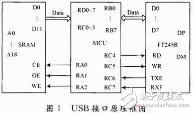
The USB interface is designed with a single chip microcomputer and FT245R as the core device. The principle is shown in Figure 1. Since the FT245R integrates high-speed signals involving the USB protocol all within the chip, the system's performance requirements for the microcontroller are reduced. This design selects Microchip's mid-range microcontroller PIC16F877, which has a maximum operating clock of 20 MHz, five parallel I/O ports, and 13 interrupt sources, which fully meet the requirements for simultaneous control of the FT245R and the storage test system.

In Figure 1, the SRAM is a static memory integrated in the memory test system. After the test process, the SRAM is full of test data. The MCU acts as a bridge in the USB interface. The PORTD of the I/O port and the lower four bits of the PORTC are connected to the 12 b data bits in the SRAM as a data bus. Similarly, the PORTB port of the microcontroller is connected to the 8b data bit in the F245R to become another data bus. The three control signals related to the access operation in the SRAM are connected to RA0, RA1 and RA2 of the microcontroller respectively, and the four control signals related to the data transfer of the FT245R are connected to the upper four bits of the PORTC port of the microcontroller. In the hardware design, the two data buses are different. The data bus from the SRAM to the microcontroller is unidirectional, and data can only be transferred from the memory to the microcontroller. The data bus between the MCU and the FT245R is bidirectional, which can complete the uplink transmission of the test data and complete the downlink transmission of the computer command.
In addition, the storage test system is powered by a battery. In order to save limited power, the USB interface circuit can adopt a computer-powered method. The USB port of the computer can provide 5 V power supply, and the maximum load current can reach 500 mA, which can fully meet the power requirements of the USB interface designed in this paper.

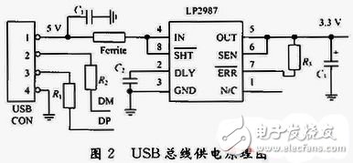
Figure 2 is a schematic diagram of the USB bus power supply. The 5 V power supply is output from the 1-pin of the USB port. After being filtered by the capacitor C1 and ferrite, it enters the DC-DC converter LP2987. After voltage conversion, it outputs 3.3 V DC voltage (load current 200 mA), and supplies the MCU and FT245R. And its peripheral components.
200*300mm Hydrogel Screen Protector
Made of TPU material imported from South Korea, it can effectively protect the screen from unnecessary wear or scratches and reduce the impact of falling.
The flexible material design allows the Screen Protector to adapt to the contours of any device, so it can be connected to curved displays and rounded edges. The Full-Cover Screen Protector can perfectly fit your screen and provide maximum protection.
The oleophobic coating technology protects the glass from fingerprints left by sweat and grease, and fully supports the 3D touch function on the iPad.
The ultra-transparent thickness of 0.14mm ensures the sensitivity of the original touch screen. When using Apple Pencil, it can still maintain a high touch sensitivity. 99% transparency provides an ideal natural viewing experience.
If you want to know more about Imported Screen Protector For iPad products, please click the product details to view the parameters, models, pictures, prices and other information about Imported Screen Protector For iPad.
Whether you are a group or an individual, we will try our best to provide you with accurate and comprehensive information about the Imported Screen Protector For iPad!
Screen Protector For iPad, Imported Screen Protector, 200*300 Screen Protector, Imported Protective Film, iPad Screen Protector,Imported Hydrogel Film
Shenzhen Jianjiantong Technology Co., Ltd. , https://www.jjttpucuttingplotter.com