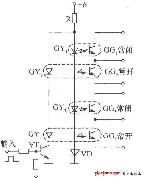
As shown in the figure is a switch circuit with two normally open contacts (contacts) and two normally closed contacts. When the input signal is low level "0", the transistor VT is turned off, and the light-emitting diode GY2 in the photocoupler No current flows with GY4, the phototransistors GG2 and GG4 are not conducting, which is equivalent to the switch being disconnected, which is called a normally open contact, and the current flows in the light-emitting diodes GY1 and GY3, making the phototransistors GG1 and GG3 conductive, equivalent When the switch is closed, it is called normally closed contact. When the input signal is high level "1", the transistor VT is turned on, and the current flows in GY2 and GY4, and the corresponding GG2 and GG4 are turned on, which is equivalent to the switch is turned on, at this time flowing through GY2 and GY4 The current of R produces a large voltage drop on R. Because GY1, GY3 and diode VD are connected in series, the current flowing through GY1 and GY3 is very small and does not emit light. GG1 and GG3 are cut off, which is equivalent to a switch off. In this way, it acts as a double-pole double-throw switch. If the two photocouplers above or below are omitted in the figure, it becomes a single-pole double-throw switch, and if two more photocouplers are added in the corresponding positions, it becomes a three-pole double-throw switch.

The figure shows a switch circuit diagram with two normally open contacts (contacts) and two normally closed contacts
Game Touch Screen Thumb,Gaming Rgb Keyboard,Gaming Bluetooth Mouse,Gaming Bluetooth Keyboard
MICROBITS TECHNOLOGY LIMITED , https://www.microbitstrade.com