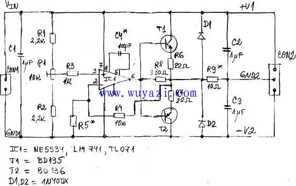
Voltage divider circuit diagrams using op amps and bipolar junction transistors If the load is variable or not symmetrical, the voltage dividers shown in Figures 3 and 4 may not work well. In order to solve this problem, sometimes we will use a voltage divider based on a single op amp (such as TL071, OPA134, NE5534/A or LM741) and additional complementary bipolar junction transistors (such as PN2222A+PN2907A, BD135+BD136, etc.). . Figure 5 shows an example of such a voltage divider. 
Figure 5: A simple voltage divider designed with op amps and bipolar junction transistors.
The output voltage is regulated with P1. This voltage divider works like a DC amplifier with a gain Av equal to Av = 1 + R4 / R5. R5 can be omitted if it is not needed, and the gain at this time is unit 1. This circuit can also be used as a follower and current buffer.
The output current of the voltage divider is limited to 50mA to 2000mA, depending on the output capabilities of transistors T1 and T2 and the op amp. Capacitor C4* is only used when external frequency compensation is required for the op amp. Most audio power amplifiers include all of the components shown in Figure 5, making them ideal for building adjustable and non-adjustable voltage dividers.
Shenzhen Xcool Vapor Technology Co.,Ltd , https://www.szxcoolvape.com