Analog and digital wiring are the same
Bypass or decoupling capacitor
Both analog and digital devices require these types of capacitors when routing. They need to be connected to a capacitor near their power supply pins. This capacitor is typically 0.1mF. Another type of capacitor is required on the system power supply side. Typically, this capacitor is approximately 10mF.
The locations of these capacitors are shown in Figure 1. The capacitance range is between 1/10 and 10 times the recommended value. However, the pins must be short and should be as close as possible to the device (for 0.1mF capacitors) or to the power supply (for 10mF capacitors).
Adding bypass or decoupling capacitors to the board and the location of these capacitors on the board are common sense for both digital and analog designs. But the interesting thing is that the reasons are different. In analog wiring designs, bypass capacitors are typically used to bypass high-frequency signals on the power supply. If no bypass capacitors are added, these high-frequency signals may enter the sensitive analog chip through the power supply pins. In general, the frequency of these high frequency signals exceeds the ability of analog devices to reject high frequency signals. If a bypass capacitor is not used in the analog circuit, noise may be introduced into the signal path, and even more severe conditions may cause vibration.
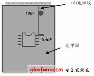
Figure 1 In analog and digital PCB designs, bypass or decoupling capacitors (1mF) should be placed as close as possible to the device. The power supply decoupling capacitor (10mF) should be placed at the power line inlet of the board. In all cases, the pins of these capacitors should be short
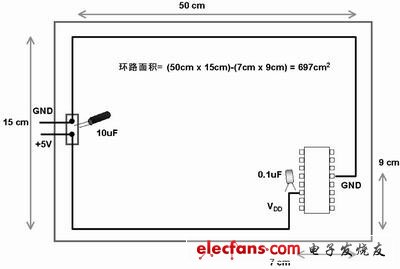
Figure 2 On this board, different routes are used to route the power and ground lines. Due to this improper fit, the electronic components and lines of the board are more likely to be electromagnetically interfered.
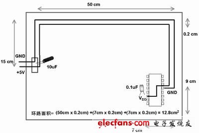
Figure 3 In this single panel, the power and ground wires to the devices on the board are close together. The matching of the power and ground wires in this board is more appropriate than in Figure 2. The possibility of electromagnetic interference (EMI) in electronic components and circuits in the board is reduced by 679/12.8 times or about 54 times
For digital devices such as controllers and processors, decoupling capacitors are also required, but for different reasons. One function of these capacitors is to act as a "mini" charge bank. In digital circuits, switching the gate state typically requires a large current. It is advantageous to have additional "standby" charge due to switching transient currents on the chip and flowing through the board during switching. If there is not enough charge when performing the switching action, the power supply voltage will change greatly. A voltage change that is too large can cause the digital signal level to go into an indeterminate state and is likely to cause the state machine in the digital device to malfunction. The switching current flowing through the board trace will cause a voltage change, and the board trace has parasitic inductance. The voltage change can be calculated by the following formula: V = LdI/dt
Where V = voltage change; L = board trace inductance; dI = current flow through the trace; dt = current change time.
Therefore, it is preferable to apply a bypass (or decoupling) capacitor at the power supply or at the power supply pin of the active device for a variety of reasons.
Power cord and ground wire are to be put together
The position of the power cord and the ground wire are well matched to reduce the possibility of electromagnetic interference. If the power and ground wires are not properly matched, a system loop is designed and noise is likely to occur. An example of a PCB design with improper power and ground wiring is shown in Figure 2.
On this board, the designed loop area is 697cm2. With the method shown in Figure 3, the possibility of radiated noise on the board or outside the board inducing a voltage in the loop can be greatly reduced.
Lead Free Piezoelectric Elements
The Co-Al Co-doped Barium Titanate
Lead-free Piezoelectric Ceramics was successfully developed by Yuhai company
through repeated experiments. By Researching the influence of Co-Al Co-doping
on the structure and properties of Barium Titanate-based piezoelectric
ceramics, the formulation and preparation technology of Barium Titanate-based
piezoelectric ceramics were optimized. Yuhai`s BaTiO3 was prepared by conventional
solid-phase sintering method, with the piezoelectric constant d33 (>170pC/N),
dielectric loss tgδ≤0.5% and mechanical coupling coefficient Kp≥0.34.
Barium titanate lead-free piezoelectric
ceramics are important basic materials for the development of modern science
and technology, which was widely used in the manufacture of ultrasonic
transducers, underwater acoustic transducers, electroacoustic transducers,
ceramic filters, ceramic transformers, ceramic frequency discriminators, high
voltage generators, infrared detectors, surface acoustic wave devices,
electro-optic devices, ignition and detonation devices, and piezoelectric
gyroscope and so on.
Application: military, ocean, fishery, scientific research,
mine detection, daily life and other fields.
China Patent of Yuhai company`s BaTiO3
Chinese Patent No.: ZL 2011 1
0126758.6
Name: Lead-free Barium Titanate
Piezoelectric Material with Addition of Cobalt and Aluminum
Lead free piezo material BaTiO3
Lead-free Material
Properties
BaTiO3
Dielectric Constant
ɛTr3
1260
Coupling factor
KP
0.34
K31
0.196
K33
0.43
Kt
0.32
Piezoelectric coefficient
d31
10-12m/v
-60
d33
10-12m/v
160
g31
10-3vm/n
-5.4
g33
10-3vm/n
14.3
Frequency coefficients
Np
3180
N1
2280
N3
Nt
2675
Elastic compliance coefficient
Se11
10-12m2/n
8.4
Machanical quality factor
Qm
1200
Dielectric loss factor
Tg δ
%
0.5
Density
Ï
g/cm3
5.6
Curie Temperature
Tc
°C
115
Young's modulus
YE11
<109N/m3
119
Poison Ratio
0.33

Piezo Element,Piezo Ceramic Elements,Piezoelectric Ceramic,Pzt Tubes
Zibo Yuhai Electronic Ceramic Co., Ltd. , https://www.yhpiezo.com