With the rapid development of technology and the application of high-resolution digital-analog hybrid circuits, the circuit design is becoming more and more complex and the precision is getting higher and higher. Therefore, the design of high-precision AD conversion circuit becomes instrumentation and various measurement control systems. Difficulties. This system is derived from the temperature control system design of instrument and instrument. It adopts high-precision, low-temperature drift high-quality analog and digital devices, supplemented by 52 series single-chip microcomputer as controller, and complex programmable logic device CPLD (Comp lex Programmable Array Logic) as frequency. The tested hardware platform implements the design of an AD converter with high resolution and low linearity error. Through this design, we master the design method of high-precision, low-drift high-end AD converter, the design of CPLD, and the hardware design and software programming of 52 series MCU.
1 system function and structure
The main purpose of the system is to design a 16-bit VFC-type AD converter that uses the integration principle to convert the input voltage (or current) into a frequency output. The frequency measurement is carried out by using a CPLD device with a high counting frequency, and the single-chip microcomputer controls the frequency measurement operation and frequency calculation of the CPLD.
To complete the AD conversion with a V/F converter, one timer and two counters are required. The counter counting frequency limits the output frequency of the V/F device. This design uses a CPLD device with a higher counting frequency and a single-chip microcomputer to form a speed measuring module. The CPLD has good versatility, avoids the dependence on the dedicated device, and reduces the risk caused by the discontinuation of the dedicated device or the emergence of the loan problem. Required control.
The VFC type AD converter pulse frequency is proportional to the input voltage, and its precision is high, the linearity is good, the conversion speed is centered, the number of conversion bits and speed is adjustable, and the connection with the CPU is the least, and the number of conversion bits is not increased. The CPU is connected, so VFC provides an inexpensive and effective solution for AD conversion technology.
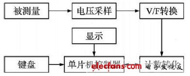
The system can be divided into a voltage sampling part, an analog-digital conversion part, and a control part. The voltage sampling part includes: a precision test voltage source. The analog-to-digital conversion section includes: voltage amplification and offset, V/F conversion module, and count conversion module. The control part includes: controller module, keyboard, display module, system principle box as shown in Figure 1.
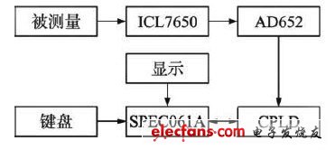
In order to realize the functions of each module, a better solution is selected: 1 precision reference source, precision low temperature drift high-grade reference source, voltage division; 2 voltage amplification and offset, operational amplifier ICL7650; 3V / F conversion, using AD652 chip 4 frequency test, using CPLD (complex programmable logic device); 5 controller, using Sunplus SPEC061A microcontroller; 6 display, using LCD screen; 7 electrical isolation, using optocoupler, the system designed as shown in Figure 2 .

Figure 1 System block diagram

Figure 2 is a system block diagram
2 system hardware design
2. 1 precision test reference source
For a 16-bit AD converter, the full-amplitude input voltage is only 100 mV. If you want to test its performance, you need a reference source with extremely high precision and very low temperature drift. The circuit principle is shown in Figure 3.
The AD586 is a high-precision 5 V reference source from AD. The temperature drift is as low as 2 10 - 6 /°C and the noise is 100 nV / Hz. The voltage is divided by a fixed resistor and an adjustable resistor to generate a voltage of 0 to 100 mV. In order to increase the load capacity of the voltage, voltage following is required. The OPA333 is a zero-drift precision op amp with a maximum drift of 0. 05μV / °C. At the same time, two 2. 5 V reference sources LM336 are used to reduce the effects of power supply fluctuations. The LM336's output current is 10 mA to meet the needs of the OPA33. The resistor for voltage division is adjustable by the pointer type of 10 turns, which can achieve the desired accuracy.

Figure 3 Schematic diagram of the reference source circuit
ZGAR PCC KIT
ZGAR electronic cigarette uses high-tech R&D, food grade disposable pod device and high-quality raw material. All package designs are Original IP. Our designer team is from Hong Kong. We have very high requirements for product quality, flavors taste and packaging design. The E-liquid is imported, materials are food grade, and assembly plant is medical-grade dust-free workshops.
From production to packaging, the whole system of tracking, efficient and orderly process, achieving daily efficient output. We pay attention to the details of each process control. The first class dust-free production workshop has passed the GMP food and drug production standard certification, ensuring quality and safety. We choose the products with a traceability system, which can not only effectively track and trace all kinds of data, but also ensure good product quality.
We offer best price, high quality Vape Device, E-Cigarette Vape Pen, Disposable Device Vape,Vape Pen Atomizer, Electronic cigarette to all over the world.
Much Better Vaping Experience!


ZGAR PCC KIT E-Cigarette Vape Pen,ZGAR PCC KIT Disposable Device Vape,PCC SET,ZGAR PCC KIT Vape Pen Atomizer,ZGAR PCC KIT Disposable E-Cigarette OEM vape pen,ZGAR PCC KIT electronic cigarette
Zgar International (M) SDN BHD , https://www.zgarpods.com