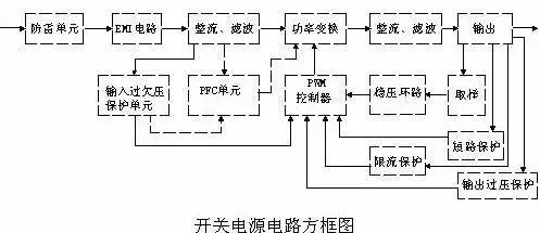
The main circuit of the switching power supply is composed of an input electromagnetic interference filter (EMI), a rectification and filtering circuit, a power conversion circuit, a PWM controller circuit, and an output rectification and filtering circuit. The auxiliary circuit has an input over-voltage protection circuit, an output over-voltage protection circuit, an output over-current protection circuit, and an output short-circuit protection circuit.
The circuit block diagram of the switching power supply is as follows:
1, AC input rectifier filter circuit principle:
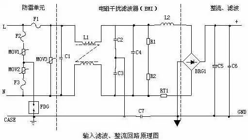
1. Lightning protection circuit: When there is lightning strike and high voltage is generated through the power grid, the circuit consists of MOV1, MOV2, MOV3: F1, F2, F3 and FDG1. When the voltage applied across the varistor exceeds its working voltage, its resistance decreases, so that the high-voltage energy is consumed on the varistor. If the current is too large, F1, F2, and F3 will burn and protect the latter circuit.
2. Input filter circuit: The double π-type filter network composed of C1, L1, C2 and C3 mainly suppresses the electromagnetic noise and clutter signals of the input power source, prevents interference to the power supply, and also prevents high-frequency miscellaneous generated by the power supply itself. Waves interfere with the grid. When the power is turned on, the C5 should be charged. Because the instantaneous current is large, adding RT1 (thermistor) can effectively prevent the inrush current. Since the instantaneous energy is completely consumed on the RT1 resistor, the RT1 resistance decreases after the temperature rises after a certain time (RT1 is a negative temperature coefficient component), at which time the energy consumed is very small, and the latter circuit can work normally. 3. Rectifier filter circuit: After the AC voltage is rectified by BRG1, it is filtered by C5 to obtain a relatively pure DC voltage. If the C5 capacity becomes smaller, the output AC ripple will increase. 2, DC input filter circuit principle:
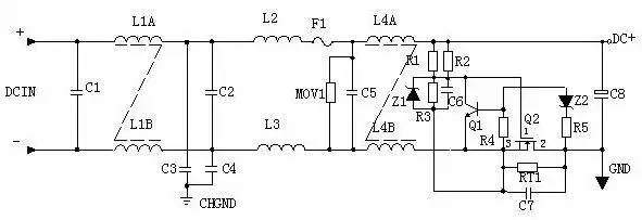
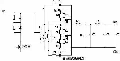
1. Input filter circuit: The double π-type filter network composed of C1, L1 and C2 mainly suppresses the electromagnetic noise and clutter signals of the input power source to prevent interference to the power supply, and also prevents the high-frequency clutter generated by the power supply itself. Grid interference. C3 and C4 are safety capacitors, and L2 and L3 are differential mode inductors.
2. R1, R2, R3, Z1, C6, Q1, Z2, R4, R5, Q2, RT1, and C7 form an anti-surge circuit. At the moment of starting, due to the presence of C6, Q2 is not conducting, and the current forms a loop through RT1. Q2 turns on when the voltage on C6 is charged to the regulated value of Z1. If the C8 leakage or the short circuit of the latter stage is short, the voltage drop generated by the current on RT1 increases at the moment of starting, Q1 is turned on so that the gate voltage of Q2 is not turned on, and RT1 will burn out in a short time. Protect the rear stage circuit.
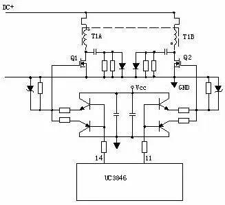
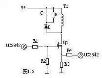
Third, the power conversion circuit1, MOS tube works:
At present, the most widely used insulated gate field effect transistor is a MOSFET (MOS transistor), which works by utilizing the electroacoustic effect of the semiconductor surface. Also known as surface field effect devices. Since its gate is in a non-conducting state, the input resistance can be greatly improved up to 105 ohms. The MOS transistor uses the magnitude of the gate-source voltage to change the amount of induced charge on the semiconductor surface, thereby controlling the drain current. . 2, the common schematic:
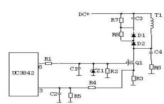
3. Working principle:
R4, C3, R5, R6, C4, D1, D2 form a buffer, and the switch MOS tube is connected in parallel, so that the voltage stress of the switch tube is reduced, EMI is reduced, and secondary breakdown does not occur. When the switch Q1 is turned off, the primary winding of the transformer is prone to spike voltage and spike current. These components combine to absorb the peak voltage and current well. The current peak signal measured from R3 participates in the duty cycle control of the current working cycle and is therefore the current limit of the current working cycle. When the voltage on R5 reaches 1V, UC3842 stops working and switch Q1 turns off immediately. The junction capacitances CGS and CGD in R1 and Q1 together form an RC network, and the charge and discharge of the capacitor directly affects the switching speed of the switching tube. If R1 is too small, it will cause oscillation and electromagnetic interference will be very large; if R1 is too large, it will reduce the switching speed of the switching tube. Z1 usually limits the GS voltage of the MOS transistor to 18V or less, thus protecting the MOS transistor. The gate controlled voltage of Q1 is saw-shaped wave. When the duty ratio is larger, the longer the Q1 conduction time is, the more energy the transformer stores. When Q1 is cut off, the transformer passes D1, D2, R5. R4 and C3 release energy and at the same time achieve the purpose of magnetic field reset, which is ready for the next storage and transmission of energy of the transformer. The IC adjusts the duty ratio of the 6-pin saw-wave according to the output voltage and current, thus stabilizing the output current and voltage of the whole machine. C4 and R6 are spike voltage absorption loops. 4. Push-pull power conversion circuit:
Q1 and Q2 will turn on in turn.
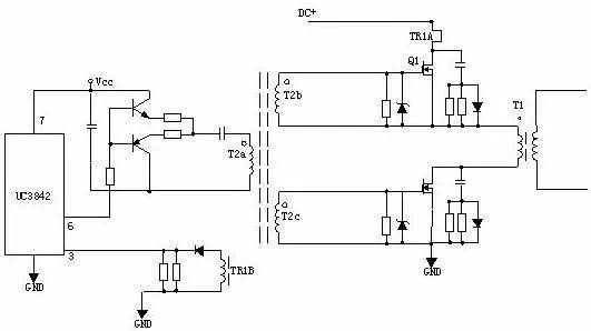
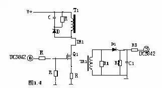
5. Power conversion circuit with drive transformer:
T2 is the drive transformer, T1 is the switching transformer, and TR1 is the current loop.
1. Forward rectifier circuit:
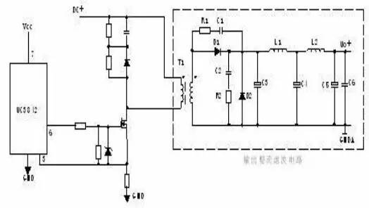
T1 is a switching transformer whose phase of the primary and secondary poles is in phase. D1 is a rectifier diode, D2 is a freewheeling diode, and R1, C1, R2, and C2 are sharp peak circuits. L1 is a freewheeling inductor, and C4, L2, and C5 form a π-type filter.
2. Flyback rectifier circuit:
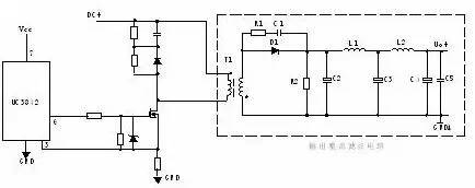
T1 is a switching transformer with opposite phases of the primary and secondary poles. D1 is a rectifier diode, and R1 and C1 are sharp peak circuits. L1 is a freewheeling inductor, R2 is a dummy load, and C4, L2, and C5 form a π-type filter.
3. Synchronous rectifier circuit:
Working principle: When the upper end of the transformer is positive, the current is turned on by C2, R5, R6 and R7, the circuit forms the loop, and Q2 is the rectifier. The gate of Q1 is turned off due to the reverse bias. When the lower end of the secondary of the transformer is positive, the current is turned on by C3, R4, and R2, and Q1 is a freewheeling tube. The Q2 gate is turned off due to the reverse bias. L2 is a freewheeling inductor, and C6, L1, and C7 form a π-type filter. R1, C1, R9, and C4 are sharp peak circuits.
Fifth, the principle of the voltage regulation loop1. Feedback circuit schematic:
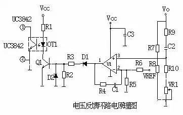
2, working principle:
When the output U0 rises, after the voltage is divided by the sampling resistors R7, R8, R10, VR1, the voltage of the U13 pin rises. When it exceeds the reference voltage of the U12 pin, the U11 pin outputs a high level, so that Q1 is turned on, and the optocoupler OT1 emits light. When the diode emits light and the phototransistor is turned on, the potential of the UC38421 pin becomes lower, which changes the output duty ratio of the U16 pin and reduces U0. When the output U0 decreases, the U13 pin voltage decreases. When it is lower than the U12 pin reference voltage, the U11 pin outputs a low level, Q1 does not conduct, the optocoupler OT1 LED does not emit light, the phototransistor does not conduct, and the UC38421 pin potential rises. High, thus changing the U16 pin output duty cycle increases, U0 decreases. Repeatedly to keep the output voltage stable. Adjusting VR1 changes the output voltage value. The feedback loop is an important circuit that affects the stability of the switching power supply. Such as feedback resistor capacitance error, leakage, virtual soldering, etc., will produce self-oscillation, the fault phenomenon is: waveform abnormality, empty, full load oscillation, output voltage instability.
Sixth, short circuit protection circuit1. In the case of short circuit at the output terminal, the PWM control circuit can limit the output current to a safe range. It can implement the current limiting circuit in various ways. When the power limiting current does not work when it is short-circuited, only another Add a part of the circuit. 2, short circuit protection circuit usually has two kinds, the following figure is a small power short circuit protection circuit, the principle is as follows:
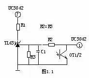
When the output circuit is short-circuited, the output voltage disappears, the optocoupler OT1 is not turned on, the voltage of the UC38421 pin rises to about 5V, the voltage divider of R1 and R2 exceeds the TL431 reference, making it turn on, the VCC potential of the UC38427 pin is pulled low, and the IC stops working. . After UC3842 stops working, the potential of 1 foot disappears, TL431 does not turn on the potential of UC38427, and UC3842 restarts, and it starts again. When the short circuit disappears, the circuit can automatically return to normal operation.
3. The figure below is a medium power short circuit protection circuit. The principle is as follows:
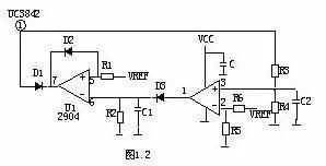
When the output is short-circuited, the UC38421 pin voltage rises, and the U13 pin potential is higher than the 2 pin. The comparator flips the 1 pin output high potential to charge C1. When the voltage across C1 exceeds the 5 pin reference voltage, the U17 pin outputs a low potential, UC38421 pin. Below 1V, UCC3842 stops working, the output voltage is 0V, and the circuit starts again. When the short circuit disappears, the circuit works normally. R2 and C1 are charge and discharge time constants, and short circuit protection does not work when the resistance value is incorrect.
4. The figure below is a common current limiting and short circuit protection circuit. Its working principle is briefly described as follows:
When the output circuit is short-circuited or over-current, the primary current of the transformer increases, the voltage drop across R3 increases, the voltage of the 3-pin increases, and the output duty of the UC38426 pin gradually increases. When the voltage of the 3-pin exceeds 1V, the UC3842 turns off and no output. .
5. The following figure is a protection circuit for sampling current with a current transformer. It has low power consumption, but the cost is high and the circuit is more complicated. The working principle is as follows:
If the output circuit is short-circuited or the current is too large, the voltage induced by the secondary winding of TR1 is higher. When the UC38423 pin exceeds 1 volt, the UC3842 stops working and repeats. When the short circuit or overload disappears, the circuit recovers itself.
Seven, the output current limit protection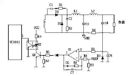
The figure above is a common output current limiting protection circuit. Its working principle is as shown in the above figure: When the output current is too large, the voltage across RS (manganese copper wire) rises, the voltage of U13 pin is higher than the reference voltage of 2 feet, U11 foot The output high voltage, Q1 is turned on, the optocoupler has a photoelectric effect, the voltage of the UC38421 pin is lowered, and the output voltage is lowered, thereby achieving the purpose of output overload current limiting.
Eight, the principle of output overvoltage protection circuitThe function of the output overvoltage protection circuit is to limit the output voltage to a safe value when the output voltage exceeds the design value. When the internal voltage regulation loop of the switching power supply fails or the output overvoltage phenomenon is caused by improper operation of the user, the overvoltage protection circuit protects to prevent damage to the power equipment of the latter stage. The most common overvoltage protection circuits are as follows: 1. SCR trigger protection circuit:
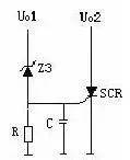
As shown above, when the Uo1 output rises and the Zener diode (Z3) breaks through, the control terminal of the SCR1 (SCR1) gets the trigger voltage, so the SCR is turned on. The Uo2 voltage is shorted to ground, and the overcurrent protection circuit or the short circuit protection circuit will work to stop the operation of the entire power supply circuit. When the output overvoltage phenomenon is eliminated, the control terminal trigger voltage of the thyristor is discharged to the ground through R, and the thyristor is restored to the off state.
2. Photoelectric coupling protection circuit:
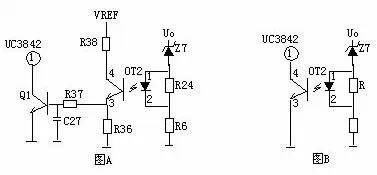
As shown above, when Uo has an overvoltage phenomenon, the Zener diode breaks through and conducts current through the optocoupler (OT2) R6 to the ground, and the light-emitting diode of the photocoupler emits light, thereby making the phototransistor of the photocoupler through. The base of Q1 is electrically turned on, and the 3-pin power of 3842 is reduced, so that the IC is turned off, the operation of the entire power supply is stopped, Uo is zero, and the cycle is repeated.
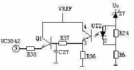
3. Output voltage limiting protection circuit:
The output voltage limiting protection circuit is as shown in the figure below. When the output voltage rises, the Zener diode turns on the optocoupler, the Q1 base has a driving voltage and the pass, the UC38423 voltage rises, the output decreases, and the Zener diode does not conduct, UC38423 The voltage is lowered and the output voltage is raised. Repeatedly, the output voltage will settle within a range (depending on the regulator voltage).
4, the output overvoltage lockout circuit:
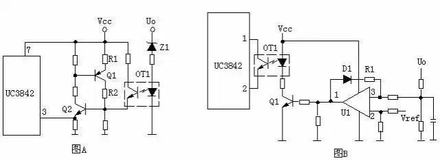
The working principle of Figure A is that when the output voltage Uo rises, the Zener diode is turned on, the optocoupler is turned on, and the base of Q2 is electrically turned on. Since the base voltage of Q2 is turned on, the base voltage is also turned on, and the Vcc voltage is R1. Q1, R2 make Q2 always on, UC38423 pin is always high and stops working. In Figure B, UO raises the U13 pin voltage and pin 1 outputs a high level. Due to the presence of D1 and R1, the U11 pin always outputs a high level. Q1 is always on, and the UC38421 pin is always low and stops working. . Positive feedback?
Nine, power factor correction circuit (PFC)1. Schematic diagram:
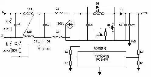
2, working principle:
The input voltage is EMI filter composed of L1, L2, L3, etc., BRG1 rectifies one way to send PFC inductor, and the other way is divided by R1 and R2 and then sent to PFC controller as sampling of input voltage to adjust the duty of control signal. Ratio, that is, change the turn-on and turn-off time of Q1 to stabilize the PFC output voltage. L4 is a PFC inductor that stores energy when Q1 is on and applies energy when Q1 is off. D1 is the start diode. D2 is a PFC rectifier diode, C6, C7 filter. The PFC voltage is sent to the subsequent stage circuit, and the other circuit is divided by R3 and R4 and sent to the PFC controller as the sampling of the PFC output voltage to adjust the duty ratio of the control signal and stabilize the PFC output voltage.
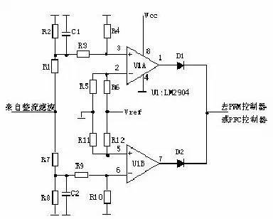
Ten, input overvoltage protection1, schematic:
2, working principle:
The input and undervoltage protection principles of the AC input and DC input switching power supplies are approximately the same. The sampling voltage of the protection circuit is derived from the input filtered voltage. The sampling voltage is divided into two ways. One is divided into R1, R2, R3 and R4 and then input to the comparator 3 pin. If the sampling voltage is higher than the reference voltage of the 2 pin, the comparator 1 pin outputs a high level to control the main controller. Shutdown, no output from the power supply. The other way is divided into R6, R8, R9, R10 and then input to the comparator 6 pin. If the sampling voltage is lower than the 5 pin reference voltage, the comparator 7 pin outputs a high level to control the main controller to turn off, and the power supply has no output. .
Plug Terminal Block,Screw Terminal Plug,Terminal Block Plug And Socket,Plug In Terminal Block Connector
Cixi Zhongyi Electronics Factory , https://www.cx-zhongyi.com